Studying Unique Alloy Allies for Better Device Technology
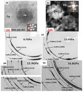
Better alloys lead to better devices. Additive manufacturing allows engineers to make finely tuned alloys with previously unattainable combinations of properties. Typically, increased strength would decrease ductility and electrical conductivity. But additive manufacturing can create materials that break the old rules. Here, researchers from University of Michigan, LLNL and ANL used the U.S. Department of Energy's Advanced Photon Source (APS) to look at an alloy of copper (Cu) and iron (Fe) under extremely high pressures. Normally, copper and iron don’t mix. But the additive manufacturing technique studied by the researchers allowed distinct layers of copper and iron to remain side-by-side, even as they structurally transformed under pressures as high as 20 gigapascals (GPa). Their results, published in the journal nanomaterials, confirmed computational models of iron and copper alloys, and show how to precisely tailor alloys at high pressures. The team used direct-metal deposition additive manufacturing to create a Cu50Fe50 alloy tailored for use in high-pressure environments.
The high pressure would put the material under a great deal of strain, and potentially reveal unexpected combinations of strength, ductility, or atomic arrangements. The researchers used the direct deposition manufacturing technique to create a layered structure. One layer was iron with precisely placed bits of copper in it; the other layer was copper containing precisely placed bits of iron (Fig. 1.). The study also showed that, while many of the material transformations predicted by computational studies really did occur, they only occurred in small, localized regions of the metal, on the scale of nanometers. They did not occur to the metal in bulk, which is quite surprising and new information.
The team used direct-metal deposition additive manufacturing to create a Cu50Fe50 alloy tailored for use in high-pressure environments. The high pressure would put the material under a great deal of strain, and potentially reveal unexpected combinations of strength, ductility, or atomic arrangements. The researchers used the direct deposition manufacturing technique to create a layered structure. One layer was iron with precisely placed bits of copper in it; the other layer was copper containing precisely placed bits of iron (Fig. 1.) The study also showed that, while many of the material transformations predicted by computational studies really did occur, they only occurred in small, localized regions of the metal, on the scale of nanometers. They did not occur to the metal in bulk, which is quite surprising and new information.
See: Arya Chatterjee1, Dmitry Popov2, Nenad Velisavljevic2,3, and Amit Misra1**, “Phase Transitions of Cu and Fe at Multiscales in an Additively Manufactured Cu–Fe Alloy under High-Pressure,” Nanomater. 12, 1514. (2022). DOI: 10.3390/nano12091514
Author affiliations: 1University of Michigan, 2Argonne National Laboratory, 3Lawrence Livermore National Laboratory