Forming a new semiconductor nanostructure by compressing lead chalcogenide nanocrystals
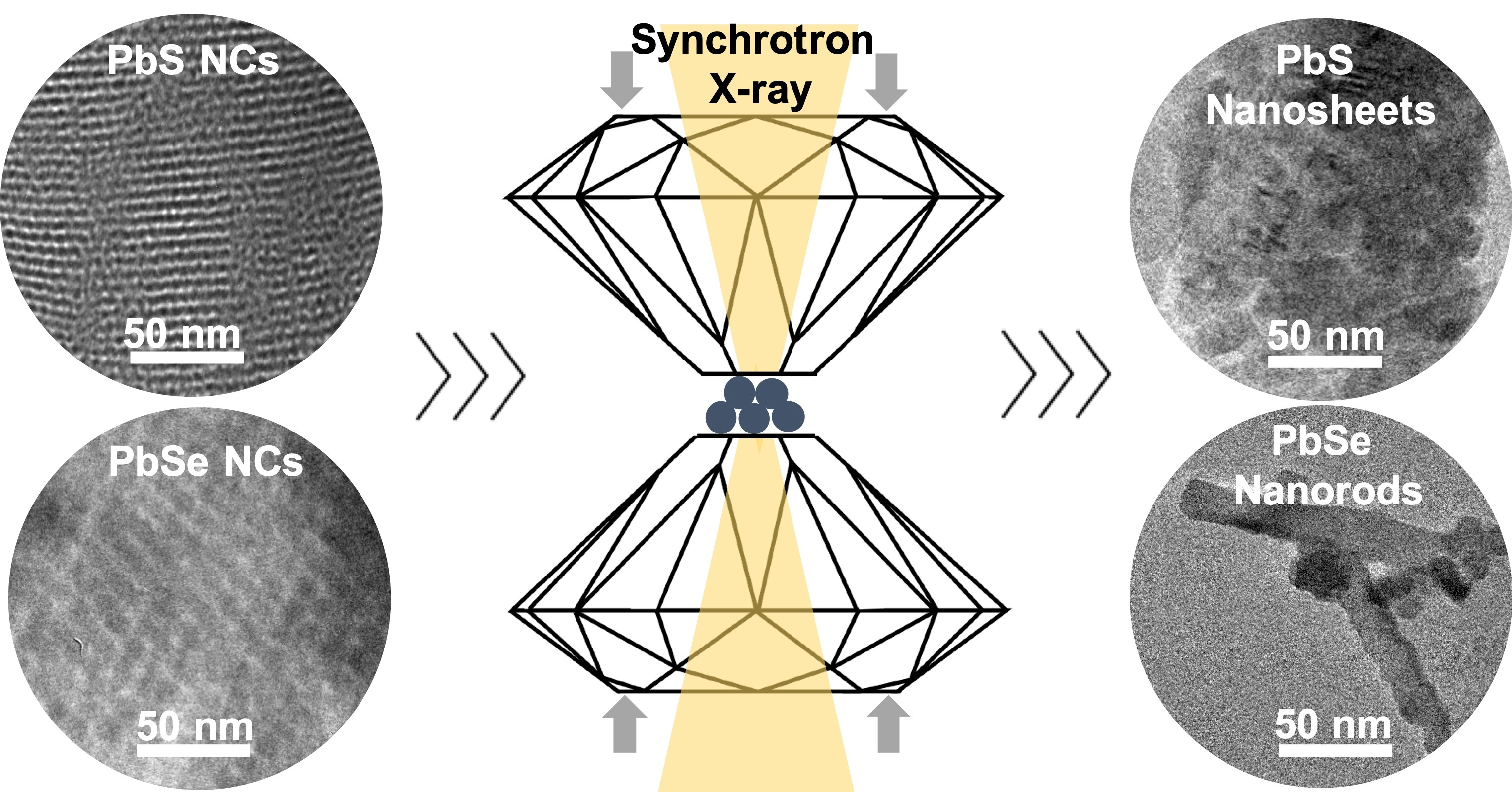
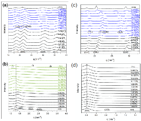
Pressure-induced assembly has promising applications for fabrication of nanostructured materials from a wide range of nanocrystals with various size, shape, and composition. Using diamond-anvil compression techniques, combined with small/wide angling x-ray scattering and the x-ray diffraction tools at the Advanced Photon Source under remote operations, the team was able to characterize the structural and morphological changes in PbS and PbSe semiconductor nanocrystals. The experiments performed at HPCAT -16IDD and 16BMD demonstrated that the applied pressure induces a reversible atomic phase transition of the nanocrystals under a hydrostatic pressure. Additionally, over a certain threshold pressure, the nanocrystals are forced to contact and coalesce, forming new semiconductor nanostructures. High Resolution Transmission Electron Microscopy revealed the formation of single crystalline two-dimensional nanosheets and one-dimensional nanorods through pressure-induced mesoscale coalescence of the nanocrystal PbS and PbSe. This study showed that through pressure-induced nanocrystal phase transition, materials engineering and synthesis becomes remarkably flexible.
See: Lingyao Meng, Sakun Duwal, J.Matthew D. Lane, Tommy Ao, Brian Stoltzfus, Marcus Knudson, Kevin Austin, Changyong Park, Paul Chow, Yuming Xiao, Hongyou Fan, Yang Qin, "Pressure Induced Assembly and Coalescence of Lead Chalcogenide Nanocrystals," J. Am. Chem. Soc. 143 (7), 2688-2693 (2021). DOI: 10.1021/jacs.0c13350